- 您现在的位置:买卖IC网 > Sheet目录484 > NOIV1SE025KA-GDC (ON Semiconductor)IC IMAGE SENSOR 25MP 355PGA
�� �
�
�NOIV1SN025KA�
�Frame� N�
�Frame� N+1�
�Exposure� State�
�FOT�
�Reset�
�Integrating�
�FOT�
�Reset�
�Integrating�
�FOT�
�Readout�
�FOT�
�FOT�
�FOT�
�Image� Array� Global� Reset�
�fr_length�
�exposure�
�=� ROT�
�=� Readout�
�Figure� 18.� Integration� Control� for� Pipelined� Global� Shutter� Mode� (Master,� fr_mode� =� 0x0)�
�Frame� N�
�Frame� N+1�
�Exposure� State�
�FOT�
�Reset�
�Integrating�
�FOT�
�Reset�
�Integrating�
�FOT�
�Readout�
�FOT�
�FOT�
�FOT�
�Image� Array� Global� Reset�
�exposure� x� mult_timer�
�fr_length� x� mult_timer�
�=� ROT�
�=� Readout�
�Figure� 19.� Integration� Control� for� Pipelined� Global� Shutter� Mode� (Master,� fr_mode� =� 0x1)�
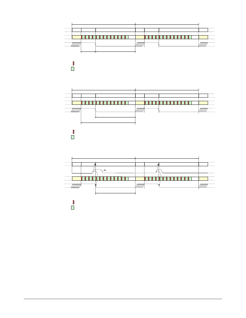
�Frame� N�
�Frame� N+1�
�Exposure� State�
�FOT�
�Reset�
�Integrating�
�FOT�
�Reset�
�Integrating�
�FOT�
�trigger0�
�(No� effect� on� falling� edge� )�
�Readout�
�FOT�
�FOT�
�FOT�
�Image� Array� Global� Reset�
�exposure� x� mult_timer�
�=� ROT�
�=� Readout�
�Figure� 20.� Exposure� Time� Control� in� Triggered� Global� Mode� (Master)�
�Triggered� Global� Shutter� (Slave)�
�Exposure� or� integration� time� is� fully� controlled� by� means�
�starts� during� a� frame� readout.� Therefore,� the� effective�
�time� during� which� the� image� core� is� in� a� reset� state� is�
�of� the� trigger� pin� in� slave� mode.� The� register� ’s� fr_length,�
�exposure,� and� mult_timer� are� ignored� by� the� sensor.�
�A� rising� edge� on� the� trigger� pin� indicates� the� start� of� the�
�exposure� time,� while� a� falling� edge� initiates� the� transfer� and�
�readout� of� the� image� array.� In� other� words,� the� high� time� of�
�the� trigger� pin� indicates� the� integration� time,� the� period� of�
�the� trigger� pin� indicates� the� frame� time.�
�The� use� of� the� trigger� during� slave� mode� is� shown� in�
�Figure� 21.�
�NOTES:�
�?� The� start� of� the� exposure� time� is� synchronized� to� the�
�start� of� a� new� line� (during� ROT)� if� the� exposure� period�
�?�
�?�
�extended� to� the� start� of� a� new� line.�
�If� the� trigger� is� deasserted� before� the� end� of� readout,� the�
�exposure� time� is� extended� until� the� end� of� the� last�
�active� line.� Consequently� the� FOT� and� start� of� frame�
�readout� is� postponed� accordingly.�
�The� trigger� pin� needs� to� be� kept� low� during� the� FOT.�
�The� monitor� pins� can� be� used� as� a� feedback� to� the�
�FPGA/controller� (eg.� use� monitor0,� indicating� the� very�
�first� line� when� monitor_select� =� 0x5� ?� a� new� trigger� can�
�be� initiated� after� a� rising� edge� on� monitor0).�
�http://onsemi.com�
�25�
�发布紧急采购,3分钟左右您将得到回复。
相关PDF资料
NP100P04PDG-E1-AY
MOSFET P-CH -40V MP-25ZP/TO-263
NP100P04PLG-E1-AY
MOSFET P-CH -40V MP-25ZP/TO-263
NP100P06PDG-E1-AY
MOSFET P-CH -60V MP-25ZP/TO-263
NP100P06PLG-E1-AY
MOSFET P-CH -60V MP-25ZP/TO-263
NP109N04PUJ-E1B-AY
MOSFET N-CH 40V MP-25ZP/TO-263
NP109N055PUJ-E1B-AY
MOSFET N-CH 55V MP-25ZP/TO-263
NP110N03PUG-E1-AY
MOSFET N-CH 30V MP-25ZP/TO-263
NP110N04PDG-E1-AY
MOSFET N-CH 40V MP-25ZP/TO-263
相关代理商/技术参数
NOIV1SE1300A-QDC
功能描述:图像传感器和彩色传感器 VITA 1300 1.3 Mpx 150FPS Globl Shutter RoHS:否 制造商:Avago Technologies 类型:Color Sensors 工作电源电压:2.5 V 封装 / 箱体: 图象大小: 颜色读出:Color 最大工作温度:+ 70 C 最小工作温度:- 25 C 封装:Reel
NOIV1SE1300A-QXC
制造商:ONSEMI 制造商全称:ON Semiconductor 功能描述:VITA 1300 1.3 Megapixel 150 FPS Global Shutter CMOS Image Sensor
NOIV1SE1300A-XDC
制造商:ONSEMI 制造商全称:ON Semiconductor 功能描述:VITA 1300 1.3 Megapixel 150 FPS Global Shutter CMOS Image Sensor
NOIV1SE1300A-XXC
制造商:ONSEMI 制造商全称:ON Semiconductor 功能描述:VITA 1300 1.3 Megapixel 150 FPS Global Shutter CMOS Image Sensor
NOIV1SE2000A-QDC
功能描述:IC IMAGE SENSOR 2.3MP 52LLC RoHS:是 类别:传感器,转换器 >> 图像,相机 系列:* 标准包装:480 系列:- 象素大小:6.7µm x 6.7µm 有源象素阵列:768H x 488V 每秒帧数:52 电源电压:3.3V 类型:CMOS 成像 封装/外壳:48-QFP 供应商设备封装:48-QFP 包装:托盘 请注意:* 配用:4H2105-ND - HEADBOARD FOR KAC-004014H2104-ND - KIT EVAL FOR KAC-00401 其它名称:4H20954H2095-NDKAC-00401-CBC-LB-A0
NOIV1SE5000A
制造商:ONSEMI 制造商全称:ON Semiconductor 功能描述:VITA 5000 5.3 Megapixel 75 FPS Global Shutter CMOS Image Sensor
NOIV1SE5000A-QDC
功能描述:图像传感器和彩色传感器 VITA 5000 5.3 Mpx 75FPS Global Shutter RoHS:否 制造商:Avago Technologies 类型:Color Sensors 工作电源电压:2.5 V 封装 / 箱体: 图象大小: 颜色读出:Color 最大工作温度:+ 70 C 最小工作温度:- 25 C 封装:Reel
NOIV1SN025KA-GDC
功能描述:IC IMAGE SENSOR 25MP 355PGA RoHS:是 类别:传感器,转换器 >> 图像,相机 系列:* 标准包装:480 系列:- 象素大小:6.7µm x 6.7µm 有源象素阵列:768H x 488V 每秒帧数:52 电源电压:3.3V 类型:CMOS 成像 封装/外壳:48-QFP 供应商设备封装:48-QFP 包装:托盘 请注意:* 配用:4H2105-ND - HEADBOARD FOR KAC-004014H2104-ND - KIT EVAL FOR KAC-00401 其它名称:4H20954H2095-NDKAC-00401-CBC-LB-A0